
In high-voltage, high-frequency power conversion systems, busbar parasitic parameters have a decisive impact on the dynamic stress of switching devices and the overall system EMI characteristics. High-precision laminated busbars and shunts are not merely structural conductive components in the traditional sense, but rather precision power interconnect assemblies engineered based on low-inductance lamination topology and distributed capacitive coupling principles. The core design philosophy lies in stacking multiple thin copper layers and vacuum-laminating them with high-dielectric-strength (>40 kV/mm) insulating films to achieve an extremely low effective loop area. This configuration physically maximizes the cancellation of mutual inductance between conductors, reducing stray inductance (ESL) to the nanohenry (nH) range. Simultaneously, the inherent interlayer parasitic capacitance (typically ranging from several nanofarads to microfarads) functions as a natural RC snubber network embedded directly into the main current path, providing in-situ clamping against di/dt spikes (up to several kA/μs) generated during IGBT/SiC MOSFET turn-off transients, thereby optimizing the switching trajectory and voltage safety operating area (SOA) of the power module at the source.
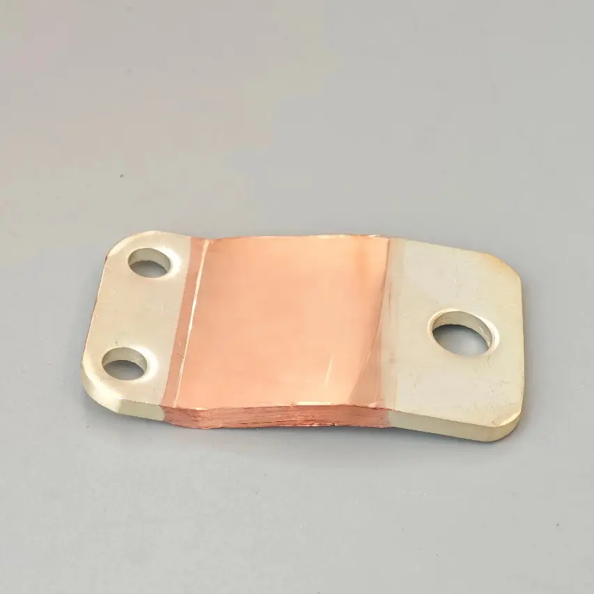
The manufacturing of this component involves cross-process coordination of precision sheet metal forming, high-cleanliness lamination, and high-accuracy CNC bending. The base material is high-conductivity oxygen-free copper (Cu-ETP, IACS conductivity ≥101%), processed through multi-station progressive dies for one-step blanking of terminal functional areas, ensuring hole-to-hole positional tolerances are controlled within ±0.05 mm to meet current-sharing requirements for parallel-connected power modules. To address the skin effect under high-frequency currents, some designs employ multiple thin copper layers in parallel to increase the effective current-carrying surface area. The core lamination process is carried out in a Class 10,000 cleanroom environment, where a high-temperature vacuum hot press applies a precisely controlled pressure-temperature profile (e.g., heating rate ≤3°C/min, holding pressure ≥3.5 MPa) to copper layers coated with polyimide (PI) or polyethylene naphthalate (PEN) insulating films, ensuring complete resin flow and filling of microscopic gaps to eliminate the risk of partial discharge. Subsequently, multi-axis CNC bending centers are utilized to achieve complex 3D spatial bends, with precise spring-back compensation to ensure installation conformance across X/Y/Z axes within the cabinet. Finally, selective plating with silver (Ag) or nickel-under-tin treatment is applied to maintain contact resistance stable at the micro-ohm level, complemented by 100% hipot (dielectric withstand) testing and insulation resistance verification, guaranteeing long-term creep and thermo-mechanical fatigue life under harsh environments such as salt spray and temperature-humidity cycling.
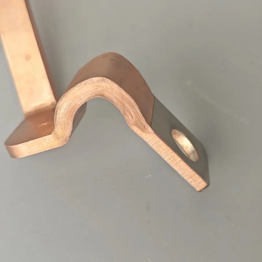
In summary, choosing high-precision laminated copper busbars delivers transformative upgrades to your system. In terms of electrical performance, their ultra-low stray inductance reduces loop inductance by over 70% while effectively suppressing harmful IGBT voltage spikes, providing rock-solid protection for sensitive power modules and significantly extending system service life. At the same time, superior electromagnetic compatibility stems from the inherent filtering effect of the precision interlayer capacitance structure, dramatically reducing electromagnetic interference (EMI) and helping your equipment pass stringent EMC certification with ease. From an engineering application perspective, a single integrated laminated link replaces dozens of bulky, difficult-to-manage cables, dramatically simplifying cabinet layouts and reducing total assembly time by more than 50%. The ultra-compact copper-insulation micro-interconnections ensure extremely short thermal paths, enabling lower temperature rise under high loads while unlocking higher current-carrying capacity. Finally, 100% customizable terminal configurations, precise mounting hole matrices, and complex 3D bending angles deliver true plug-and-play integration, completely eliminating human wiring errors during field deployment—making this the ideal choice for building highly competitive power electronics systems.
Post time: Aug-28-2026